Ultrafast Laser Fabrication for Microelectronics in 2025: Market Dynamics, Technology Innovations, and Strategic Forecasts. Explore Key Growth Drivers, Regional Hotspots, and Competitive Insights for the Next 5 Years.
- Executive Summary & Market Overview
- Key Technology Trends in Ultrafast Laser Fabrication
- Market Size, Segmentation, and Growth Forecasts (2025–2030)
- Competitive Landscape and Leading Players
- Regional Analysis: Opportunities and Market Leaders by Geography
- Challenges, Risks, and Emerging Opportunities
- Future Outlook: Strategic Recommendations and Investment Insights
- Sources & References
Executive Summary & Market Overview
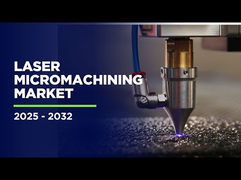
Ultrafast laser fabrication is an advanced manufacturing technique that utilizes extremely short laser pulses—typically in the femtosecond (10-15 s) to picosecond (10-12 s) range—to process materials with exceptional precision and minimal thermal damage. In the context of microelectronics, this technology enables the direct writing, patterning, drilling, and structuring of materials at micro- and nanoscale dimensions, supporting the ongoing miniaturization and complexity of electronic devices.
The global market for ultrafast laser fabrication in microelectronics is poised for robust growth in 2025, driven by escalating demand for high-performance, miniaturized electronic components in sectors such as consumer electronics, automotive, telecommunications, and healthcare. According to MarketsandMarkets, the ultrafast laser market is projected to reach USD 3.5 billion by 2025, with microelectronics representing a significant and rapidly expanding application segment.
Key market drivers include the proliferation of advanced packaging technologies (such as 3D integration and system-in-package), the need for precise microvia drilling in printed circuit boards (PCBs), and the fabrication of microelectromechanical systems (MEMS). Ultrafast lasers are increasingly favored over traditional photolithography and mechanical processing due to their ability to achieve sub-micron resolution, high aspect ratios, and superior edge quality without inducing heat-affected zones. This results in higher device reliability and yield, which are critical for next-generation microelectronic products.
Geographically, Asia-Pacific dominates the market, led by manufacturing powerhouses such as China, South Korea, and Taiwan, where investments in semiconductor fabrication and advanced electronics manufacturing are accelerating. North America and Europe also maintain strong positions, supported by ongoing R&D and the presence of leading technology firms and equipment suppliers, including TRUMPF, Coherent, and amcoss.
Looking ahead to 2025, the ultrafast laser fabrication market in microelectronics is expected to benefit from continued innovation in laser sources, beam delivery systems, and process automation. Strategic collaborations between laser manufacturers, semiconductor foundries, and research institutions are anticipated to further accelerate the adoption of ultrafast laser technologies, enabling new device architectures and manufacturing paradigms.
Key Technology Trends in Ultrafast Laser Fabrication
Ultrafast laser fabrication is rapidly transforming the microelectronics sector, driven by the demand for miniaturization, higher performance, and advanced packaging. In 2025, several key technology trends are shaping the adoption and evolution of ultrafast laser processes in microelectronics manufacturing.
- Femtosecond and Picosecond Laser Processing: The shift from nanosecond to femtosecond and picosecond lasers is enabling unprecedented precision in material ablation and structuring. These ultrashort pulse lasers minimize thermal damage, allowing for the fabrication of intricate features on substrates such as silicon, glass, and flexible polymers. This is particularly critical for next-generation integrated circuits and MEMS devices, where feature sizes continue to shrink TRUMPF Laser.
- 3D Micro- and Nano-Structuring: Ultrafast lasers are increasingly used for direct-write 3D structuring, enabling the creation of complex microelectronic components such as through-silicon vias (TSVs), microchannels, and embedded passive devices. This capability supports advanced packaging and heterogeneous integration, which are essential for high-performance computing and AI chips Laser Focus World.
- Wafer Dicing and Scribing: Ultrafast laser dicing is replacing traditional mechanical and diamond saw methods, offering higher yields, cleaner edges, and reduced kerf loss. This is especially valuable for fragile or thin wafers used in power electronics and photonics. The adoption of stealth dicing and laser grooving is expected to accelerate in 2025 Hamamatsu Photonics.
- Integration with Automation and AI: The integration of ultrafast laser systems with AI-driven process control and advanced robotics is enhancing throughput and consistency. Real-time monitoring and adaptive process optimization are reducing defects and enabling mass production of complex microelectronic devices MarketsandMarkets.
- Green and UV Ultrafast Lasers: The development of green (515 nm) and deep-UV ultrafast lasers is expanding the range of processable materials, including transparent and wide-bandgap semiconductors. This trend is crucial for emerging applications in optoelectronics and advanced sensor platforms Coherent.
These trends underscore the pivotal role of ultrafast laser fabrication in enabling the next wave of innovation in microelectronics, supporting both established and emerging applications in 2025 and beyond.
Market Size, Segmentation, and Growth Forecasts (2025–2030)
The global market for ultrafast laser fabrication in microelectronics is poised for robust expansion between 2025 and 2030, driven by escalating demand for miniaturized, high-performance electronic components. Ultrafast lasers—characterized by pulse durations in the picosecond and femtosecond range—enable precise material processing with minimal thermal damage, making them indispensable for advanced microelectronics manufacturing.
According to MarketsandMarkets, the ultrafast laser market (encompassing applications in microelectronics, medical devices, and materials processing) was valued at approximately USD 1.5 billion in 2023, with microelectronics accounting for a significant share. Projections indicate a compound annual growth rate (CAGR) of 12–15% for ultrafast laser applications in microelectronics through 2030, outpacing the broader laser market due to the sector’s rapid innovation cycles and increasing adoption in semiconductor fabrication, wafer dicing, and advanced packaging.
Segmentation within the ultrafast laser fabrication market for microelectronics can be analyzed by:
- Laser Type: Femtosecond lasers dominate due to their superior precision, but picosecond lasers are gaining traction for cost-sensitive, high-throughput applications.
- Application: Key segments include semiconductor wafer processing, via drilling, thin-film patterning, and microelectromechanical systems (MEMS) fabrication. The semiconductor wafer processing segment is expected to maintain the largest share, fueled by the transition to sub-10 nm nodes and 3D integration technologies.
- Geography: Asia-Pacific leads the market, with China, South Korea, and Taiwan at the forefront of semiconductor manufacturing investments. North America and Europe follow, driven by R&D and the presence of major microelectronics OEMs.
Growth drivers for 2025–2030 include the proliferation of 5G/6G devices, artificial intelligence (AI) hardware, and the Internet of Things (IoT), all of which require increasingly complex and miniaturized microelectronic components. Additionally, the push for advanced packaging and heterogeneous integration is accelerating the adoption of ultrafast laser processes for high-precision interconnects and defect-free dicing.
Challenges remain, such as high capital costs and the need for skilled operators, but ongoing advancements in laser source efficiency and automation are expected to mitigate these barriers. Overall, the ultrafast laser fabrication market for microelectronics is set for dynamic growth, with revenues projected to surpass USD 3 billion by 2030, according to IDTechEx.
Competitive Landscape and Leading Players
The competitive landscape of the ultrafast laser fabrication market for microelectronics in 2025 is characterized by a mix of established photonics giants, specialized laser system manufacturers, and innovative startups. The sector is driven by the increasing demand for high-precision, high-throughput manufacturing processes in semiconductor device fabrication, advanced packaging, and microelectromechanical systems (MEMS) production.
Key players dominating this space include TRUMPF Group, Coherent Corp., and IPG Photonics, all of which have made significant investments in ultrafast (femtosecond and picosecond) laser technologies tailored for microelectronics applications. These companies offer integrated solutions that combine high-power ultrafast lasers with advanced beam delivery and process monitoring systems, enabling precise micromachining, wafer dicing, and via drilling with minimal thermal damage.
Emerging players such as Light Conversion and Amplitude Laser are gaining traction by focusing on compact, high-repetition-rate femtosecond lasers optimized for industrial integration. Their systems are increasingly adopted for applications like glass cutting for display panels and selective material removal in advanced packaging.
The competitive dynamics are further shaped by strategic partnerships between laser manufacturers and semiconductor equipment suppliers. For example, TRUMPF Group has collaborated with leading semiconductor foundries to co-develop process modules for next-generation chip architectures, while Coherent Corp. has expanded its portfolio through acquisitions and joint ventures targeting the microelectronics sector.
- Innovation Focus: Leading players are investing heavily in R&D to improve pulse control, beam shaping, and real-time process feedback, aiming to address the stringent requirements of sub-micron feature fabrication and heterogeneous integration.
- Regional Competition: While Europe and the US host many of the technology leaders, Asian companies—particularly in Japan, South Korea, and China—are rapidly scaling up their capabilities, supported by strong demand from local semiconductor and display manufacturers (MarketsandMarkets).
- Barriers to Entry: High capital requirements, the need for deep application expertise, and the importance of long-term customer relationships create significant barriers for new entrants.
Overall, the ultrafast laser fabrication market for microelectronics in 2025 is marked by intense competition, rapid technological advancement, and a clear trend toward vertical integration and application-specific system development.
Regional Analysis: Opportunities and Market Leaders by Geography
The regional landscape for ultrafast laser fabrication in microelectronics is shaped by varying levels of technological adoption, investment in semiconductor manufacturing, and the presence of key industry players. In 2025, Asia-Pacific (APAC) continues to dominate the market, driven by robust semiconductor manufacturing ecosystems in countries such as China, South Korea, Taiwan, and Japan. These nations benefit from strong government support, significant R&D investments, and the presence of leading foundries and electronics manufacturers. For instance, TSMC and Samsung Electronics are leveraging ultrafast laser systems to achieve higher precision in wafer dicing, via drilling, and advanced packaging, which are critical for next-generation microelectronics.
North America remains a significant market, propelled by innovation hubs in the United States and Canada. The region’s focus on advanced research, coupled with the presence of major technology companies and research institutions, fosters the adoption of ultrafast laser fabrication. Companies such as Applied Materials and Lumentum are at the forefront, integrating ultrafast laser solutions into microelectronics manufacturing to enhance throughput and yield. The U.S. government’s initiatives to bolster domestic semiconductor production, as outlined in the CHIPS Act, further stimulate demand for advanced fabrication technologies.
Europe is characterized by a strong emphasis on precision engineering and photonics research. Germany, France, and the Netherlands are notable for their contributions, with companies like TRUMPF and ASML developing ultrafast laser systems tailored for microelectronics applications. The European Union’s strategic investments in semiconductor sovereignty and photonics innovation, as highlighted in the European Chips Act, are expected to create new opportunities for market growth and collaboration across the region.
- Asia-Pacific: Market leadership driven by high-volume manufacturing, government incentives, and the presence of global foundries.
- North America: Opportunities in R&D, prototyping, and advanced packaging, supported by policy initiatives and leading technology firms.
- Europe: Growth potential in precision applications, photonics integration, and collaborative R&D projects.
Overall, regional opportunities in ultrafast laser fabrication for microelectronics are closely tied to the maturity of local semiconductor industries, government policies, and the innovation capacity of market leaders. Strategic partnerships and cross-border collaborations are expected to further accelerate technology adoption and market expansion in 2025.
Challenges, Risks, and Emerging Opportunities
Ultrafast laser fabrication is increasingly pivotal in the microelectronics sector, enabling high-precision patterning, drilling, and structuring at micro- and nanoscale levels. However, the adoption of this technology in 2025 faces several challenges and risks, even as new opportunities emerge.
One of the primary challenges is the high capital expenditure required for ultrafast laser systems. These systems, which utilize femtosecond or picosecond pulses, demand advanced optical components and precise control mechanisms, leading to significant upfront costs. This can be a barrier for small and medium-sized enterprises (SMEs) seeking to enter the market or upgrade existing fabrication lines (Laser Focus World).
Another risk involves process integration. Ultrafast laser fabrication must be seamlessly integrated with existing semiconductor manufacturing workflows, which are often optimized for traditional photolithography and etching techniques. Incompatibilities can result in yield losses or require costly process requalification (SEMI). Additionally, the thermal effects, though minimized in ultrafast regimes, can still induce microcracks or unwanted material modifications if not carefully controlled.
Supply chain vulnerabilities also pose a risk. The specialized components required for ultrafast lasers—such as high-quality crystals, precision optics, and advanced cooling systems—are often sourced from a limited number of suppliers. Disruptions, whether due to geopolitical tensions or raw material shortages, can impact production timelines and costs (MarketsandMarkets).
Despite these challenges, several emerging opportunities are driving market optimism. The push for advanced packaging, heterogeneous integration, and miniaturization in microelectronics is creating demand for the unique capabilities of ultrafast lasers, such as selective material removal and 3D structuring. Furthermore, the rise of compound semiconductors and flexible electronics opens new application areas where traditional fabrication methods fall short (IDTechEx).
In summary, while ultrafast laser fabrication in microelectronics faces notable financial, technical, and supply chain risks in 2025, the technology’s ability to address next-generation device requirements positions it for significant growth, especially as process integration and cost barriers are gradually overcome.
Future Outlook: Strategic Recommendations and Investment Insights
The future outlook for ultrafast laser fabrication in microelectronics is shaped by rapid technological advancements, evolving end-user requirements, and intensifying competition among equipment manufacturers. As the industry moves into 2025, several strategic recommendations and investment insights emerge for stakeholders seeking to capitalize on this dynamic market.
Strategic Recommendations:
- Focus on Integration with Advanced Packaging: The shift toward heterogeneous integration and advanced packaging in microelectronics is accelerating demand for precise, high-throughput laser processes. Companies should invest in R&D to tailor ultrafast laser systems for through-silicon via (TSV) drilling, redistribution layer (RDL) patterning, and wafer-level packaging, aligning with trends highlighted by Yole Group.
- Expand Application Portfolio: Beyond traditional dicing and drilling, ultrafast lasers are increasingly used for selective material removal, microstructuring, and defect repair. Diversifying application offerings can help capture emerging opportunities in MEMS, photonics, and flexible electronics, as noted by Laser Focus World.
- Leverage AI and Automation: Integrating AI-driven process control and real-time monitoring can enhance yield and reduce downtime. Investment in smart manufacturing solutions will be critical for differentiation, as emphasized by SEMI.
- Strengthen Supply Chain Resilience: The global semiconductor supply chain remains vulnerable to disruptions. Strategic partnerships with component suppliers and localizing key manufacturing steps can mitigate risks, a priority underscored by McKinsey & Company.
Investment Insights:
- Growth Hotspots: Asia-Pacific, particularly China, Taiwan, and South Korea, will continue to drive demand for ultrafast laser systems due to robust semiconductor manufacturing investments (SEMI).
- M&A and Partnerships: Expect increased merger and acquisition activity as established players seek to acquire niche technology providers and expand their ultrafast laser portfolios (Laser Focus World).
- Sustainability: Investors should prioritize companies developing energy-efficient, low-waste laser processes, aligning with ESG trends and regulatory pressures (Yole Group).
In summary, the ultrafast laser fabrication market for microelectronics in 2025 will reward innovation, agility, and strategic investment in advanced applications, automation, and supply chain resilience.
Sources & References
- MarketsandMarkets
- TRUMPF
- Coherent
- amcoss
- Laser Focus World
- Hamamatsu Photonics
- IDTechEx
- IPG Photonics
- Amplitude Laser
- Lumentum
- ASML
- McKinsey & Company